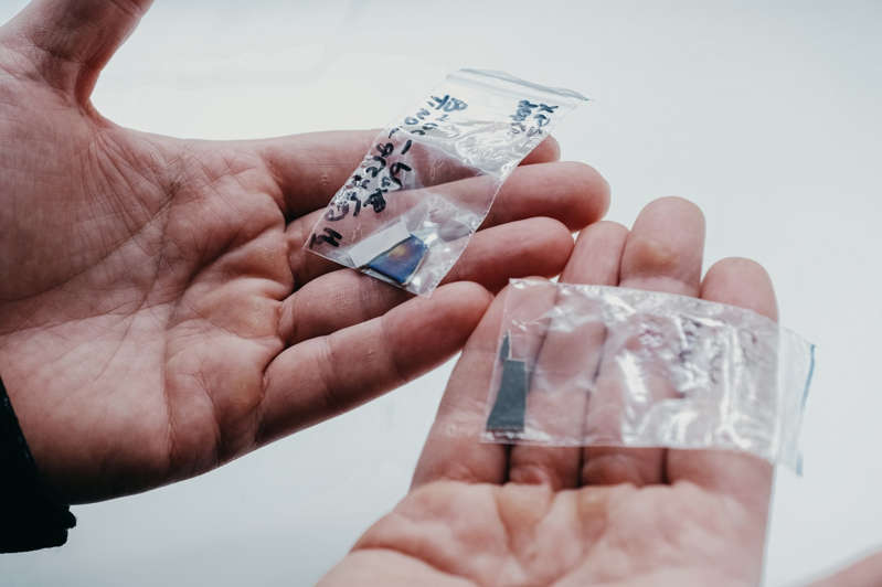
Copper-doped titanium oxynitride thin films.
Krasnoyarsk scientists have obtained new promising thin films from oxygen, copper and titanium nitride. Their electrical resistance is a thousand times less than that of ordinary titanium nitride. On the basis of the material obtained, physicists discovered new properties of copper, which allow it to accumulate on the surface of films and undergo phase transitions. The results obtained can become a technological breakthrough in the development of new generation resistors and transistors. The research results are published in the journal ACS Applied Materials & Interfaces.
Thin films based on titanium nitride are widely used in various industrial and technological fields, for example, in the manufacture of silicon microprocessors and other large integrated circuits, photocatalysts, converters of solar and thermal energy into electricity, in dentistry, and even in the manufacture of domes of churches. Due to the high electromagnetic resistance and its weak temperature dependence, chemical inertness, as well as the ability to withstand high powers and temperatures, there are currently no analogues to replace them.
Scientists of the Federal Research Center “Krasnoyarsk Scientific Center of the Siberian Branch of the Russian Academy of Sciences”, Siberian Federal University and Siberian State University named after M.F. Reshetnev obtained a new material for thin films from titanium oxynitride doped with copper. It has an electrical resistance a thousand times less than that of ordinary titanium nitride. Studying the resulting compound, physicists discovered a new phenomenon of copper segregation, which was not distributed, as is customary throughout the film, but accumulated on its surface.
The discoveries of the Krasnoyarsk physicists were led by a chain of random technical errors and the study of their consequences. Initially, the researchers planned to obtain pure titanium nitride to be used to make resistors in integrated circuits. However, everything did not go according to plan. Oxygen impurities appeared in the film growth chamber. Therefore, instead of the planned pure substance, the scientists received titanium oxynitride at the output. Moreover, he possessed uncharacteristic properties. The resistance of the resulting substance turned out to be a thousand times lower than that of pure titanium oxynitride.
Oxygen trapped in the chamber became a suspect in the unusual properties of the material. To test his involvement, scientists tried to neutralize him. For this, hydrogen was introduced into the chamber before the growth of the film. He had to react with oxygen and, forming water vapor, take it out of the chamber. However, this did not bring the expected effect. The resistance of the films remained low.
Scientists continued to “investigate” this phenomenon until they found copper impurities in the films. As it turned out, the copper got into the films because of the misaligned equipment. The gas cylinder used in the installation came to scientists with a brass valve instead of stainless steel. It was from him that particles of copper flew, beaten out by the gas directly into the growth chamber. Meanwhile, the amazing discoveries are not over. The copper brought a couple more surprises with it. Its behavior turned out to be atypical: it was not distributed over the entire film, but collected on its surface and formed an additional layer. As a result, Krasnoyarsk scientists not only received new material, but also discovered a new phenomenon – copper segregation. And they did it by a relatively cheap method by the standards of modern industries.
“We have been putting this puzzle together for three years. When the resistance of the resulting titanium oxynitride was measured, it was found to be very low compared to the pure material. We were confused. They began to examine the films, and it turned out that they contain an admixture of copper. This changed our whole idea, because copper conducts electricity very well. Further research showed that instead of being evenly distributed over the film, copper began to float to the surface and accumulate there in a narrow layer of 5-10 nanometers. As a result, we discovered a new phenomenon of copper segregation. The fact that it is not stirred but pushed out is a very good help for technologists. Moreover, we accidentally caught a phase transition between the state of heavily doped copper and weakly doped copper. The transition turned out to be quite interesting from the point of view of physics. By varying the degree of doping, different types of conductivity can be obtained. In this case, in the case of heavy alloying, a semimetal with the properties of both metals and nonmetals was obtained from copper. As a result, we got the ability to create conductive layers. This can be useful in instrumentation, for example, for devices that operate at high frequencies. Therefore, this development in the future may be useful for devices that need low resistance, for example, transistors, resistors, capacitors, photocatalysts and solar-selective absorbing coatings, ”said Philip Baron, PhD, researcher at the Institute of Physics. L.V. Kirensky Federal Research Center KSC SB RAS.
Read also:
Physicists have proposed to visualize cells using nonlinear optics
Substance from controversial Saussurea will help restore bone tissue
In children with autism, the mechanisms for understanding speech and speaking are impaired in different ways
Photosensitive proteins of archaea and eukaryotes turned out to be relatives
Historians have established the exact date of birth of Boris Godunov

